Nano-imprint lithography (NIL) creates nanoscale surface structures at a fraction of photolithography cost. Sub-100nm pattern transfer using precision-engineered molds and servo-controlled uniform pressure. Both UV-cure and thermal imprinting modes supported.
KEY ADVANTAGES
Technical Highlights
01
Sub-100nm Resolution
Feature sizes below 100nm — enabling nano-LED pitch control, anti-reflection structures, diffractive optics, and semiconductor device features at far lower cost than EUV.
02
UV and Thermal Modes
UV-cure: room temperature, fast cycle. Thermal: up to 200°C, broader substrate compatibility. Process mode is recipe-selectable.
03
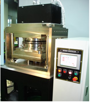
Servo-Controlled Pressure
Active uniform force across entire substrate area — critical for defect-free pattern transfer, especially near mold edges.
COMPATIBLE MATERIALS
Machinable Materials
Si Wafer (200mm, 300mm)Quartz / GlassPolymer Film (PET, PC, PMMA)SapphireGaN-on-SapphireDisplay Glass (TFT, OLED)
TECHNISCHE DATEN
Technical Specs — Two Variants
Two model variants: ANT-4 (UV photo-curing) and ANT-6H (UV + Thermal hybrid). Custom design and manufacturing available.
PATENTS
Imprint roller auto-leveling system (KR 10-2015-0072634) · Imprint device (KR 10-1408741) · KR 0522040 / US 7,140,866 B2 · KR 0585951 / US 7,202,935 B2 · PCT/KR2006/002230
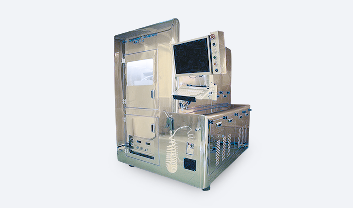
ANT-4 — UV Photo-Curing Nano Imprinting
Curing Type
UV (Ultra-Violet)
Stamp
Quartz · Si · PFPE · PDMS · PC
Wafer Size
1 ~ 4 inch
Imprinting Pressure
≤ 2 bar · Room Temperature
Imprinting Mode
Single Layer / Single Step
Imprinting Head
Chip-size Multi-Head · Multiple Fixturing / Air Chucking